script async='async' crossorigin='anonymous' src='https://pagead2.googlesyndication.com/pagead/js/adsbygoogle.js?client=ca-pub-6016566166623052'/> Verilog coding: Verilog code
Showing posts with label Verilog code. Show all posts

Thursday, 21 March 2024

Verilog Code for building an Advanced Encryption Standard (AES) Encryption Module for FPGA: A Hands-On Guide

Verilog Code for building an Advanced Encryption Standard (AES) Encryption Module for FPGA: A Hands-On Guide

In the realm of data security, the Advanced Encryption Standard (AES) stands tall as one of the most robust and widely adopted encryption algorithms. When it comes to implementing AES encryption on FPGA (Field-Programmable Gate Array) platforms, developers are presented with a unique opportunity to tailor encryption solutions to specific application requirements. In this blog post, we'll embark on a journey to design and implement an AES encryption module for FPGA, complete with step-by-step instructions and actual Verilog code snippets. Understanding AES Encryption: Before delving into the implementation details, let's briefly recap the core concepts of AES encryption. AES operates on fixed-size blocks of data, typically 128 bits, and supports key lengths of 128, 192, or 256 bits. The encryption process involves a series of transformations, including SubBytes, ShiftRows, MixColumns, and AddRoundKey, repeated for multiple rounds depending on the key size. Implementation Overview:

To implement AES encryption on FPGA, we'll break down the process into manageable steps and translate each step into Verilog code. Here's a high-level overview of the implementation process:

  1. Key Expansion: Generate round keys from the master key using the key expansion algorithm.
  2. Initial Round Processing: Perform initial transformations on the input data block.
  3. Main Round Processing: Execute multiple rounds of SubBytes, ShiftRows, MixColumns, and AddRoundKey transformations.
  4. Final Round Processing: Perform the final round of transformations without MixColumns.
  5. Integration and Testing: Integrate all AES components into a cohesive module and verify functionality through simulation and testing.


Verilog Implementation: Let's dive into the Verilog code snippets for key parts of the AES encryption module:

// Key Expansion Module module key_expansion ( input [127:0] master_key, output reg [127:0] round_keys [0:10] ); // Implementation details omitted for brevity // Generate round keys from master key // ... endmodule // Initial Round Processing Module module initial_round ( input [127:0] input_data, input [127:0] round_key, output reg [127:0] state ); // Perform initial transformations on input data block // ... endmodule // Main Round Processing Module module main_round ( input [127:0] state, input [127:0] round_key, output reg [127:0] next_state ); // Perform SubBytes, ShiftRows, MixColumns, and AddRoundKey transformations // ... endmodule // Final Round Processing Module module final_round ( input [127:0] state, input [127:0] round_key, output reg [127:0] ciphertext ); // Perform final round transformations without MixColumns // ... endmodule Designing and implementing an AES encryption module for FPGA involves a blend of cryptographic principles and hardware design considerations. By following the structured approach outlined in this blog post and leveraging Verilog for FPGA development, developers can craft efficient and secure encryption solutions tailored to specific application needs. Keywords:

  1. AES encryption,
  2. FPGA development,
  3. Verilog coding,
  4. Cryptography,
  5. Data security,
  6. Advanced Encryption Standard,
  7. Hardware design,
  8. Field-Programmable Gate Array,
  9. FPGA implementation,
  10. Verilog code,
  11. Encryption algorithms,
  12. Secure data transmission,
  13. Cryptographic modules,
  14. Cybersecurity,
  15. FPGA applications,
  16. Data protection,
  17. Embedded systems security,
  18. Hardware acceleration,
  19. Digital design,
  20. Network security

Tuesday, 21 February 2023

Verilog code for a comparator-VHDL

What is Comparator?

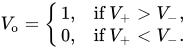
In Electronics, a comparator is used to compares two voltages (V) / Currents(I) and outputs a digital signal indicating which is larger than other. it consist of two analog input terminals  and  and one binary digital output . The output is ideally as follows

A comparator mainly has a specialized high gain Differential amplifier. Comparators are commonly used in devices that measure and digitize two analog signals, for example analog to digital signals (ADCs), as well as oscillators.

Verilog code for a 2 bit -comparator-VHDL

There are many different types of comparators. But, Here we have designed and implemented a simple 2bit-comparator which has two 2 bit inputs and three output bits these outputs says, whether one of the input is less ,greater or equal to the second input.

A 2-bit comparator is a device that compares 2-binary numbers, each of two bits and produces as one number is equal(=) or greater than (>) or less than (<) the other.


A simple 2-bit Comparator device is designed and implemented in VHDL/ Verilog Code.


The 2-bit comparator specifications are as follows:

  • Inputs: 2-bit A and B for comparison.
  • Output:
    • A>B: high if A > B else low
    • A=B: high if A = B else low
    • A<B: high if A<B else low
  • The Truth bale for 2-bit Comparator is given Below 

K-map


Equations For 2-bit Comparator


Circuit Diagrams

This is the Verilog code for the 2bit-comparator:

 // Verilog code for 2-bit comparator   
 module 2bit-comparator(input [1:0] A,B, output A-equal-B, A-less-B, A-greater-B);  
 wire w0,w1,w2,w3,w4,w5,w6,w7;  
 // A equal B output   
 xnor x1(w0,A[1],B[1]);  
 xnor x2(w1,A[0],B[0]);  
 and x3(A-equal-B,w0,w1);  
 // A < B output   
 assign w2 = (~A[0])& (~A[1])& B[0];  
 assign w3 = (~A[1])& B[1];  
 assign w4 = (~A[0])& B[1]& B[0];  
 assign A-less-B = w2 | w3 | w4;  
 // A > B output   
 assign w5 = (~B[0])& (~B[1])& A[0];  
 assign w6 = (~B[1])& A[1];  
 assign w7 = (~B[0])& A[1]& A[0];  
 assign A-greater-B = w5 | w6 | w7;  
 endmodule   
 `timescale 10 ps/ 10 ps     
 // Verilog test-bench code for 2-bit comparator   
 module test_comparator;  
 reg [1:0] A, B;  
 wire A-less-B, A-equal-B, A-greater-B;  
 integer i;   
 comparator dutt(A,B,A-less-B, A-equal-B, A-greater-B);  
initial begin for (i=0;i<4;i=i+1) begin A = i; B = i + 1; #20; end for (i=0;i<4;i=i+1) begin A = i; B = i; #20; end for (i=0;i<4;i=i+1) begin A = i+1; B = i; #20; end end endmodule

2 bit comparator logic diagram,

Monday, 23 January 2023

Carry Save Adder Verilog Code

 What is Carry Save Adder?

A Carry Save Adder (CSA) is a type of digital circuit that performs fast, parallel addition of multiple binary numbers. It is also known as a Ripple-Carry Adder (RCA) because the carry from one bit position to the next "ripples" through the entire adder. The circuit diagram for a CSA typically includes multiple full adders, which are connected in a specific way to allow for parallel addition. The verilog code for a CSA will depend on the specific design of the circuit, but it will typically include code for the full adders as well as logic for the carry-in and carry-out bits.


A Carry Save Adder circuit is typically composed of multiple full adder circuits connected in a specific way to allow for parallel addition. A full adder circuit typically includes three inputs (A, B, and Cin) and two outputs (Sum and Cout). In a Carry Save Adder, the full adders are connected such that the A and B inputs of each full adder are connected to the corresponding bit positions of the numbers being added, and the Cin input of each full adder is connected to the Cout output of the previous full adder. The Sum outputs of all the full adders are then combined to form the sum of the numbers being added, and the Cout outputs are combined to form the carry out.

fpga verilog code example,

Here is an example of verilog code for a 4-bit Carry Save Adder:


module CSA_4bit (A, B, Ci, S, Co); input [3:0] A, B; input Ci; output [3:0] S; output Co; wire Ci_1, Ci_2, Ci_3; full_adder FA0 (A[0], B[0], Ci, S[0], Ci_1); full_adder FA1 (A[1], B[1], Ci_1, S[1], Ci_2); full_adder FA2 (A[2], B[2], Ci_2, S[2], Ci_3); full_adder FA3 (A[3], B[3], Ci_3, S[3], Co); endmodule


Note that in this example, the full_adder module is assumed to be a standard full adder module with input ports for A, B, Cin and output ports for Sum and Cout.

It is worth mentioning that Carry Save Adder is a parallel adder and it's output is not a single sum but two separate parts, one is the sum and the other is the carry out. It is used in specific situations where the carry out is also needed and not only the sum.

Sunday, 26 April 2020

Ripple Counter

Verilog HDL for Ripple Counter:

Here is an example of Verilog code for a ripple counter, which is a type of counter that uses a single clock input to increment the count value: 

fpga verilog code example

Example#1

module ripple_counter(input clk, input rst, output reg [3:0] count);

always @(posedge clk) begin
    if (rst)
        count <= 4'b0000;
    else
        count <= count + 1'b1;
end

endmodule


This code defines a module called "ripple_counter" that has a 4-bit output (count) and two inputs: a clock input (clk) and a reset input (rst). The always block is triggered on the rising edge of the clock input and increments the count value by 1 on each rising edge of the clock. The if-else statement checks the reset input, if it is high the count is reset to zero.

The output will be the count value of the ripple counter. The count value will increment every clock cycle until it reach the maximum value of the count register. It's important to note that ripple counters are not recommended for high-frequency or high-speed applications as the propagation delay of the output stage causes the output to change at different times for each bit, resulting in glitches and inaccuracies.


Example# 2

!timescale 1ns/100 ps
module Ripple-Counter_4bit (A3, A2, Al, A0, Count, Reset);
output  A3, A2, Al, A0;
input    Count, R~set;
// Instantiate complementing flip-flop
Comp_D_flip_flop F0 (A0, Count, Reset);
Comp_D_flip_flop Fl (A1, A0, Reset);
Comp_D_flip_flop F2 (A2, A1 , Reset);
Comp_D_flip_flop F3 (A3, A2, Reset);
endmodule
// Complementing flip-flop with delay
// lnput to D flip-flop = Q'
module Comp_D_flip_flop (Q, CLK, Reset);
output   Q;
Input    CLK, Reset;
reg        Q;
always @  (negedge CLK, posedge Reset)
If (Reset) Q <= 1 'b0;
else Q <= #2 ~Q;                       //Intra-assignment delay
endmodule
// Stimulus for testing ripple counter
module t_Ripple_Counter_4bit;
reg Count;
reg Reset;
wire A0, Al , A2 A3;
// Instantiate ripple oounter
Rippte_Counter_4bit M0 (A3, A2, At, A0, Count, Reset);
always
#5 Count = ~Count;
lnitial
    begin
       Count = 1'b0;
       Reset = l'bl;
      #4 Reset = l'b0;
end
initial#170 $finish;

endmodule