script async='async' crossorigin='anonymous' src='https://pagead2.googlesyndication.com/pagead/js/adsbygoogle.js?client=ca-pub-6016566166623052'/> Verilog coding: Fpga
Showing posts with label Fpga. Show all posts

Monday, 23 October 2023

FPGA vs. ASIC: What's the Difference?

FPGA vs. ASIC: What's the Difference?

In the ever-evolving landscape of digital electronics, two prominent acronyms often emerge in conversations: FPGA (Field-Programmable Gate Array) and ASIC (Application-Specific Integrated Circuit). These two technologies play vital roles in the realm of custom hardware design, but they cater to distinct needs and come with their unique sets of advantages and drawbacks. In this blog post, we'll delve into the world of FPGA vs. ASIC, exploring the differences, use cases, and the eternal debate of flexibility versus optimization.


Understanding FPGA


FPGAs, or Field-Programmable Gate Arrays, are like the chameleons of the digital hardware world. They are highly adaptable and can be programmed and reprogrammed to perform various tasks. At the heart of an FPGA lies a sea of programmable logic gates, interconnects, and memory elements. These components can be configured to create custom digital circuits, making FPGAs ideal for prototyping, development, and applications with changing requirements.


Key Features of FPGAs:


1. Flexibility: FPGAs are known for their adaptability, allowing designers to modify their functionality as needed.


2. Rapid Prototyping: They are excellent for rapid prototyping, enabling quick development and testing of custom hardware designs.


3. Reconfigurability: FPGAs can be reprogrammed, making them suitable for applications that require frequent updates or changes.


 Understanding ASIC


In contrast, ASICs, or Application-Specific Integrated Circuits, are custom-designed chips engineered for a single purpose. Unlike FPGAs, ASICs are hardwired during the manufacturing process and cannot be reprogrammed. This lack of flexibility is offset by the potential for unparalleled efficiency and performance. ASICs are used when the optimization of a specific task is paramount.


Key Features of ASICs:


1. Optimized Performance:  ASICs are tailored for maximum performance and efficiency in a dedicated function.

2. Lower Power Consumption: They often consume less power than FPGAs, which is crucial for battery-powered devices.

3. Cost-Efficiency in High Volumes: In high-volume production, ASICs can be more cost-effective than FPGAs.


FPGA vs. ASIC: The Showdown


The choice between FPGA and ASIC depends on the specific requirements of a project. Here are some considerations to help you decide:


 1. Flexibility vs. Performance:

   - If flexibility and adaptability are key, FPGAs are the way to go.

   - For unparalleled performance and efficiency in a single task, ASICs shine.


 2. Development Time:

   - FPGAs offer rapid prototyping and shorter development cycles.

   - ASIC development is a lengthier process but can result in superior performance.


3. Cost Considerations:

  - FPGAs are cost-effective for low to medium production volumes.

   - ASICs become cost-effective in high-volume production.


4. Power Consumption:

   - ASICs often consume less power than FPGAs, making them ideal for battery-powered devices.


Conclusion

The FPGA vs. ASIC debate ultimately boils down to the project's unique demands. FPGAs offer flexibility, rapid development, and adaptability, making them suitable for projects where requirements may change over time. On the other hand, ASICs offer the promise of unparalleled performance and efficiency but are best suited for applications with stable and high-volume production requirements.

Choosing between FPGA and ASIC is not a matter of one being better than the other; it's about selecting the right tool for the job at hand. As technology continues to advance, both FPGAs and ASICs will find their places in shaping our digital world, each contributing to the innovation and development of custom hardware solutions.


Keywords:

FPGA vs. ASIC,

FPGA and ASIC differences,

Advantages of FPGA,

Advantages of ASIC,

FPGA or ASIC for prototyping,

FPGA and ASIC use cases, FPGA, ASIC


What is an FPGA and How Does It Work?

What is an FPGA and How Does It Work?

Field-Programmable Gate Arrays (FPGAs) are versatile integrated circuits that have revolutionized the world of digital electronics. They offer a unique blend of flexibility and high-performance processing capabilities, making them a crucial component in various industries, from telecommunications to automotive to data centers. But what exactly is an FPGA, and how does it work? In this blog post, we'll unravel the mysteries of FPGAs, shedding light on their architecture, functioning, and the myriad of applications they serve.

Understanding FPGA Basics


At its core, an FPGA is a reconfigurable semiconductor device that can be programmed to perform specific tasks. Unlike Application-Specific Integrated Circuits (ASICs), which are hardwired for specific functions, FPGAs are programmable to execute a wide range of tasks. The heart of an FPGA is a sea of logic gates and interconnects, which can be configured to create custom digital circuits tailored to a particular application.\

FPGA Architecture


Look-Up Tables (LUTs)

One of the key components of an FPGA is the Look-Up Table (LUT). LUTs act as digital logic blocks and are the building blocks of the FPGA's reprogrammability. A LUT takes a set of input signals and produces an output based on a predefined truth table. For example, a 2-input LUT can represent any logic function with two inputs.

Configurable Interconnects

The interconnects within an FPGA are just as critical as the LUTs. These interconnections are programmable, allowing you to connect different LUTs in a multitude of ways. This flexibility is what makes FPGAs adaptable to different applications.


Programmable Routing


FPGAs have programmable routing resources that enable the establishment of connections between LUTs and other logic elements. The routing is programmed to create custom data paths and connect specific components as needed for the given application.


 How FPGAs Work


When an FPGA is programmed, a Hardware Description Language (HDL) like VHDL or Verilog is used to specify the desired functionality. The HDL code is synthesized into a netlist of digital logic components and connections. This netlist is then mapped to the FPGA's LUTs and interconnects, configuring the device to perform the desired functions.


Once programmed, FPGAs can execute complex operations in parallel, making them exceptionally fast and well-suited for tasks like signal processing, image recognition, and real-time control systems.


 Applications of FPGAs


FPGAs have found their way into numerous applications. They are commonly used in telecommunications equipment, where their reprogrammability allows for easy upgrades and adaptability to new standards. They are also employed in aerospace and automotive industries for control systems, safety features, and data processing. In data centers, FPGAs are used for acceleration of specific tasks, such as encryption and deep learning.


Conclusion


Field-Programmable Gate Arrays are remarkable devices that offer the best of both worlds: the flexibility of software and the performance of dedicated hardware. Their programmable nature makes them invaluable in today's ever-changing technological landscape. Whether you're a hardware engineer, a software developer, or simply curious about the world of electronics, FPGAs are fascinating tools to explore. As technology continues to evolve, the role of FPGAs in shaping our digital world is only set to expand, and understanding their fundamental operation is key to appreciating their potential.


Keywords,

FPGA, Field-Programmable Gate Array, FPGA architecture, LUT (Look-Up Table), Configurable interconnects, Programmable routing, HDL (Hardware Description Language),  FPGA programming, FPGA functionality,  FPGA applications,  FPGA in telecommunications,  FPGA in aerospace,  FPGA in automotive, Data center acceleration, Digital logic components, Reconfigurable semiconductor, FPGA basics, VHDL, Verilog, parallel processing


Wednesday, 14 June 2023

Cascading Muxes for Larger Multiplexing: 4x1MUX, 8x1 MUX

Cascading Muxes for Larger Multiplexing: FPGA 

Introduction to Cascading Muxes for Larger Multiplexing

Multiplexers (Muxes) are fundamental digital components used to select one out of multiple input signals based on control signals. When dealing with larger multiplexing requirements, cascading multiple smaller Muxes can be an effective approach. This technique allows us to build larger Muxes with a higher number of inputs.

Cascading Muxes involves connecting the output of one Mux to the input of another Mux, effectively creating a hierarchical structure. Each stage of Muxes reduces the selection size by half, leading to a significant reduction in the number of required control signals.

To illustrate this concept, consider an 8x1 Mux, which selects one out of eight input signals. By cascading two 4x1 Muxes, we can create an 8x1 Mux. The first stage Mux selects between four input signals, and the second stage Mux selects between the outputs of the first stage Mux.

This cascading technique can be extended to create larger Muxes by adding more stages, each with smaller Muxes. The final output is obtained by selecting the appropriate signals based on the control signals at each stage.

Implementing cascading Muxes can be achieved using hardware description languages such as Verilog or VHDL. By properly designing and connecting the inputs, outputs, and control signals, the cascaded Muxes can be synthesized and implemented on an FPGA board.

Cascading Muxes offers a scalable and efficient solution for handling larger multiplexing requirements in digital logic designs. It provides flexibility and modularity by leveraging smaller Muxes to create larger ones, reducing the complexity and improving the overall efficiency of the design.

In the next section, we will explore a sample Verilog code that demonstrates the implementation of an 8x1 Mux using two cascaded 4x1 Muxes.

Example of Verilog code for cascading 4x1 multiplexers to create a larger multiplexer, such as an 8x1 Mux:


Verilog Code:

module CascadedMux(

  input wire [2:0] select,

  input wire [7:0] data,

  output wire out

);

wire [3:0] mux1_out;

wire [3:0] mux2_out;

wire [1:0] select_mux2;

assign select_mux2 = select[1:0];

mux4to1 mux1(

  .select(select[2]),

  .data({data[7], data[6], data[5], data[4]}),

  .out(mux1_out)

);

mux4to1 mux2(

  .select(select_mux2),

  .data({data[3], data[2], data[1], data[0]}),

  .out(mux2_out)

);

mux2to1 mux3(

  .select(select[0]),

  .data({mux2_out[3], mux2_out[2]}),

  .out(out)

);

endmodule


module mux4to1(

  input wire select,

  input wire [3:0] data,

  output wire out

);

assign out = select ? data[3] : 

             select ? data[2] :

             select ? data[1] :

                      data[0];

endmodule


module mux2to1(

  input wire select,

  input wire [1:0] data,

  output wire out

);

assign out = select ? data[1] : data[0];

endmodule


Explanation of the Code:

1. The `CascadedMux` module takes a 3-bit `select` signal and an 8-bit `data` input and provides a single-bit `out` output.

2. The `mux4to1` module is defined to implement a 4x1 multiplexer. It takes a `select` signal and a 4-bit `data` input, and provides a single-bit `out` output based on the select signal.

3. The `mux2to1` module is defined to implement a 2x1 multiplexer. It takes a `select` signal and a 2-bit `data` input, and provides a single-bit `out` output based on the select signal.

4. In the `CascadedMux` module, two instances of `mux4to1` are instantiated to implement the first and second stages of the cascaded multiplexer.

5. The `mux2to1` module is instantiated to implement the final stage of the cascaded multiplexer.

6. The `select` signal is appropriately split to select the desired data inputs for each stage, and the final output is assigned to the `out` signal.


Please note that this code assumes the availability of `mux4to1` and `mux2to1` modules. You can replace these modules with your own implementation or use built-in modules provided by the FPGA board's library.


Feel free to modify the code according to your specific requirements and make any necessary connections to the FPGA board.

Friday, 26 May 2023

The Future of Computing: Can FPGA Replace CPU?

 In the ever-evolving landscape of computing, there is a constant pursuit to improve performance, efficiency, and flexibility. One emerging technology that holds promise is the Field-Programmable Gate Array (FPGA). Traditionally used as hardware accelerators, FPGAs are versatile chips that can be reprogrammed for specific tasks. This blog post explores the potential of FPGAs to replace CPUs (Central Processing Units) in the future and examines the advantages, challenges, and implications of such a transition.


Understanding FPGAs :

To grasp the potential of FPGAs, it is essential to understand their architecture and capabilities. Unlike CPUs, which are fixed-function processors, FPGAs consist of a matrix of configurable logic blocks interconnected by programmable routing resources. This unique structure allows FPGAs to be customized for specific applications by reprogramming their logic and routing configurations.

Advantages of FPGAs :

FPGAs offer several advantages over CPUs. Firstly, they can be highly parallelized, enabling them to execute multiple tasks simultaneously, making them ideal for data-intensive and parallelizable workloads. Secondly, FPGAs can provide significant performance improvements in specific domains such as artificial intelligence, machine learning, and cryptography by accelerating computations through dedicated hardware. Moreover, FPGAs are power-efficient since they can eliminate the need for executing unnecessary instructions found in CPUs, resulting in optimized energy consumption.

Challenges and Limitations :

Despite their potential, there are challenges associated with FPGA adoption. Programming FPGAs requires specialized knowledge and skills, making development more complex and time-consuming compared to traditional CPU programming. Additionally, FPGAs are generally more expensive than CPUs, limiting their widespread adoption in consumer devices. The flexibility and reprogrammability of FPGAs can also lead to increased design complexity and longer development cycles. Furthermore, FPGAs may not offer the same level of general-purpose computing performance as CPUs, making them more suitable for specific applications rather than replacing CPUs entirely.

The Hybrid Approach :

A more likely scenario is the emergence of a hybrid approach that combines the strengths of both FPGAs and CPUs. By integrating FPGAs into CPU architectures, it is possible to leverage the parallel processing capabilities of FPGAs while utilizing CPUs for general-purpose computing tasks. This hybrid model can lead to highly efficient systems, where CPUs handle traditional tasks, and FPGAs provide acceleration for specialized workloads, resulting in optimized performance and energy efficiency.


While FPGA technology shows promise in certain domains, a complete replacement of CPUs is unlikely in the near future. FPGAs are better suited for specialized tasks that benefit from parallel processing and hardware acceleration. However, with ongoing advancements in FPGA technology, increased accessibility, and the emergence of hybrid architectures, FPGAs will continue to play a significant role in the evolving landscape of computing, complementing CPUs to meet the ever-growing demands of modern applications.

Tuesday, 11 April 2023

What should be the best way to learn VLSI design

 VLSI (Very Large Scale Integration) is a field of electronics that involves the design of integrated circuits by combining thousands of transistors into a single chip. If you're interested in pursuing a career in VLSI, you'll need to acquire a range of skills related to digital design, circuit analysis, and computer programming. In this blog post, we'll discuss three important skills that are essential for VLSI engineers: protocol/algorithm implementation, timing analysis, and scripting/UNIX basics.

As an aspiring VLSI engineer, I have come to appreciate the depth and breadth of this field. From RTL design and functional, physical, and timing verification to testing, DFT, synthesis, physical design, standard cell design, and much more, VLSI engineering is a vast and complex field with many interdependent and correlated topics.

To succeed in the field of ASIC and SoC design, there are a few fundamental skills you must possess. The following are the basic things that you must know to establish a strong foundation to be a successful VLSI engineer.

  1. Logic Design: Logic design is the single most important skill that you must possess as a VLSI engineer. It is the thinking process that underlies the programming of your idea. You must be able to design a module using a minimum number of gates, minimum power, and maximum performance. This step comes higher in the design hierarchy and affects the entire flow from thereon. Therefore, it is essential to have a strong grasp of your logic design concepts. Examples of logic design include FSM design, MUX-based design, flops-latches based design, sync-async design, among others. To learn logic design, take an interesting problem statement, come up with an optimized FSM design, and try to implement the same using a minimum of resources at the gate-level.

  2. HDL/RTL/HVL Coding: The industry requires you to code and code well. There is a difference between RTL coding and C-coding, where timing comes into play. Therefore, you must learn to code in either Verilog/VHDL (I learned Verilog). With RTL, you are expressing the logic design you came up with in step 1 using a hardware language. To learn RTL coding, start coding simple modules right away, express the module behavior in RTL, and the compiler will teach you the rest. Start writing simple testbenches to verify its logic/functional correctness. Then, later learn Synthesizable RTL Coding. One step further would be learning SV, UVM, RAL, SVA, etc. to write fully automated TBs. This is a vast field in itself. If you like coding, this is for you.

  3. CMOS Fundamentals: This is highly needed in backend design/physical design and full-custom circuit design/standard cell design. But having good MOS basics is always a bonus. It is a must-need for all R&D jobs. To learn CMOS fundamentals, start designing a simple circuit like an SRAM/DRAM block, and verify its timing and functional correctness using SPICE simulations.

  4. EDA Tools: Since almost the entire VLSI flow is automated using EDA tools, it is a must to gain expertise in handling them. I have learned Cadence Virtuoso, Synopsys ICC, DC, PT, etc. It is a must for almost all backend jobs. The tools are expensive, but if you are lucky to get an internship in a semiconductor company, it is even better.

  5. Computer Architecture/Microprocessor Basics: Almost all chips designed today are ASICs/SoCs. Therefore, you must understand how the CPU is organized and how the various parts work together. You will ultimately end up working on just a single block within the CPU, but having knowledge of many blocks will help you better understand the chip and ease integration. To learn computer architecture and microprocessor basics, first learn the basic theory, then try to design and implement a single CPU component, such as an ALU or a DMA controller. Take it through the entire flow from RTL->Netlist->PD.

  6. Protocol/Algorithm implementation: As a VLSI engineer, you'll be designing chips for specific applications such as image processors, networking processors, wireless chips, and more. Therefore, it's important to understand the common on-chip protocols and implement them on hardware like FPGA. One way to learn this is to take a simple crypto algorithm like RC6 and implement it on an FPGA. Another step would be to learn AMBA protocols like AHB, APB, AXI, etc.

  7. Timing Analysis: Timing Analysis is the backbone of VLSI design. It's important to understand clocks, metastability, STA (Static Timing Analysis), and analyzing a circuit for setup and hold violations, and ways to fix them. One way to learn timing analysis is to start with STA theory. Synopsys PT/ICC is needed to generate timing reports, analyze them, and later fix those violations. If you're interested in the backend flow of VLSI, working on STA could be a good option.

  8. Scripting & UNIX basics: Scripting is essential to automate routine tasks in both the frontend and backend flow of VLSI design. In frontend flow, Perl scripting is predominantly used for regression testing, register verification, etc. In the backend flow, Tcl scripting is used to execute various commands for PD (Physical Design). Learning basic UNIX commands is also crucial. You can start learning by checking out numerous online tutorials and writing simple scripts to execute routine tasks. It's also essential to leave Windows and start using UNIX as you must know the UNIX environment well.

  9. In conclusion, VLSI engineering is a highly specialized field that requires a range of skills from digital design to programming. This blog post has discussed three essential skills for VLSI engineers, but there are many more to learn. If you're interested in pursuing a career in VLSI, it's important to keep learning and updating your skills. If you have any questions, feel free to PM the author to know more                                                                                                                                    

    What is the best way to learn FPGA professionally?

    To begin with, it is advisable to have some knowledge of C programming. However, when it comes to HDL programming, it's better to have less knowledge of C programming so that you can learn faster. This is not to discourage C programmers from learning HDL successfully, but rather to acknowledge that the two methods of coding can be confusing, especially for beginners.

    Since you have a Spartan board, you can start with some demo codes and work your way up from there. Here's how to go about it:

    1. Start with basic input/output operations such as DIP switches to LEDs.
    2. Move on to smaller projects like blinking LEDs or scrolling LEDs, which use sequential and combo logic.
    3. Once you have a good grasp of timer, delay, and sequential with combo logics, move on to FSM logics for more advanced coding skills.

    Practical examples will help you learn the basics of HDL language more effectively, so it's best to focus on hands-on exercises rather than theory. You can find demo programs for your board and study how they work. Running simulations and observing the logic on every clock change is also a good way to learn.

    It's important to have a good understanding of digital electronics as well, and you can join forums like edaboard where you can get help from experts for free. For general learning, the Spartan board is sufficient. If you have a background in C programming, Verilog may be easier for you to learn. However, if you're new to programming, VHDL may be a better choice to help you become an excellent hardware engineer.

    In conclusion, keep practicing and don't be afraid to ask for help. Good luck on your HDL programming journey!

Tuesday, 21 February 2023

Verilog code for a comparator-VHDL

What is Comparator?

In Electronics, a comparator is used to compares two voltages (V) / Currents(I) and outputs a digital signal indicating which is larger than other. it consist of two analog input terminals  and  and one binary digital output . The output is ideally as follows

A comparator mainly has a specialized high gain Differential amplifier. Comparators are commonly used in devices that measure and digitize two analog signals, for example analog to digital signals (ADCs), as well as oscillators.

Verilog code for a 2 bit -comparator-VHDL

There are many different types of comparators. But, Here we have designed and implemented a simple 2bit-comparator which has two 2 bit inputs and three output bits these outputs says, whether one of the input is less ,greater or equal to the second input.

A 2-bit comparator is a device that compares 2-binary numbers, each of two bits and produces as one number is equal(=) or greater than (>) or less than (<) the other.


A simple 2-bit Comparator device is designed and implemented in VHDL/ Verilog Code.


The 2-bit comparator specifications are as follows:

  • Inputs: 2-bit A and B for comparison.
  • Output:
    • A>B: high if A > B else low
    • A=B: high if A = B else low
    • A<B: high if A<B else low
  • The Truth bale for 2-bit Comparator is given Below 

K-map


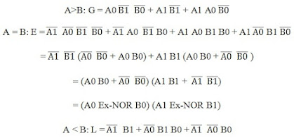
Equations For 2-bit Comparator


Circuit Diagrams

This is the Verilog code for the 2bit-comparator:

 // Verilog code for 2-bit comparator   
 module 2bit-comparator(input [1:0] A,B, output A-equal-B, A-less-B, A-greater-B);  
 wire w0,w1,w2,w3,w4,w5,w6,w7;  
 // A equal B output   
 xnor x1(w0,A[1],B[1]);  
 xnor x2(w1,A[0],B[0]);  
 and x3(A-equal-B,w0,w1);  
 // A < B output   
 assign w2 = (~A[0])& (~A[1])& B[0];  
 assign w3 = (~A[1])& B[1];  
 assign w4 = (~A[0])& B[1]& B[0];  
 assign A-less-B = w2 | w3 | w4;  
 // A > B output   
 assign w5 = (~B[0])& (~B[1])& A[0];  
 assign w6 = (~B[1])& A[1];  
 assign w7 = (~B[0])& A[1]& A[0];  
 assign A-greater-B = w5 | w6 | w7;  
 endmodule   
 `timescale 10 ps/ 10 ps     
 // Verilog test-bench code for 2-bit comparator   
 module test_comparator;  
 reg [1:0] A, B;  
 wire A-less-B, A-equal-B, A-greater-B;  
 integer i;   
 comparator dutt(A,B,A-less-B, A-equal-B, A-greater-B);  
initial begin for (i=0;i<4;i=i+1) begin A = i; B = i + 1; #20; end for (i=0;i<4;i=i+1) begin A = i; B = i; #20; end for (i=0;i<4;i=i+1) begin A = i+1; B = i; #20; end end endmodule

2 bit comparator logic diagram,

Sunday, 26 April 2020

Ripple Counter

Verilog HDL for Ripple Counter:

Here is an example of Verilog code for a ripple counter, which is a type of counter that uses a single clock input to increment the count value: 

fpga verilog code example

Example#1

module ripple_counter(input clk, input rst, output reg [3:0] count);

always @(posedge clk) begin
    if (rst)
        count <= 4'b0000;
    else
        count <= count + 1'b1;
end

endmodule


This code defines a module called "ripple_counter" that has a 4-bit output (count) and two inputs: a clock input (clk) and a reset input (rst). The always block is triggered on the rising edge of the clock input and increments the count value by 1 on each rising edge of the clock. The if-else statement checks the reset input, if it is high the count is reset to zero.

The output will be the count value of the ripple counter. The count value will increment every clock cycle until it reach the maximum value of the count register. It's important to note that ripple counters are not recommended for high-frequency or high-speed applications as the propagation delay of the output stage causes the output to change at different times for each bit, resulting in glitches and inaccuracies.


Example# 2

!timescale 1ns/100 ps
module Ripple-Counter_4bit (A3, A2, Al, A0, Count, Reset);
output  A3, A2, Al, A0;
input    Count, R~set;
// Instantiate complementing flip-flop
Comp_D_flip_flop F0 (A0, Count, Reset);
Comp_D_flip_flop Fl (A1, A0, Reset);
Comp_D_flip_flop F2 (A2, A1 , Reset);
Comp_D_flip_flop F3 (A3, A2, Reset);
endmodule
// Complementing flip-flop with delay
// lnput to D flip-flop = Q'
module Comp_D_flip_flop (Q, CLK, Reset);
output   Q;
Input    CLK, Reset;
reg        Q;
always @  (negedge CLK, posedge Reset)
If (Reset) Q <= 1 'b0;
else Q <= #2 ~Q;                       //Intra-assignment delay
endmodule
// Stimulus for testing ripple counter
module t_Ripple_Counter_4bit;
reg Count;
reg Reset;
wire A0, Al , A2 A3;
// Instantiate ripple oounter
Rippte_Counter_4bit M0 (A3, A2, At, A0, Count, Reset);
always
#5 Count = ~Count;
lnitial
    begin
       Count = 1'b0;
       Reset = l'bl;
      #4 Reset = l'b0;
end
initial#170 $finish;

endmodule

Four-bit binary counter with parallel load


Graphical Symbol of Four-bit binary counter with parallel load

Four-bit binary counter with parallel load

Functional Table of Four-bit binary counter with parallel load


fpga verilog code example
Verilog HDL of Four-bit binary counter with parallel load
module Bin-Counter-4bit-Par_Load (
output reg   [3: 0]  A-count,                    // Data output
output          C-out,                                  //Output any
input            [3: 0] Data-in,                      // Data input
input            Count,                                  //Active high to count
                      Load,                                   //Active high to load
                      CLK,                                   // Positive-edge sensitive
                      Clear                                   //Active low  
);
assign      C-out = Count & (~Load) & (A_count == 4'b111l);
always @ (posedge CLK, negedge Clear)
If (~Clear)                          A_count <= 4'b0000;
else If (Load)                      A_count <= data-in;
else If (Count)                    A_count  <= A_count + l'bl;
else                                     A_count <= A_count;            //redundant statement
endmodule


D- Flip Flop Verilog HDL

A D-  Flipflop is the simplest example of a sequential machine. Verilog HDL describes 2-positive edge D- flip-flops in two different modules. The first responds only to the clock signal Clk, the second includes an asynchronous signal reset input rst. Output Q must be declared as a register reg data type in
addition to being listed as an output. Because in a procedural assignment statement, it is a target output. The keyword posedge endures that the transfer of input D into Q is synchronized by the positive-edge transition of Clk. A change in D input at any other time does not change in Output Q.
Positive and Negative Edge D flipflop
The 2nd module includes an Asynchronous reset input, in addition to the synchronous
clk. A specific form of an if statement is used to describe such a flip-flop so that the model
can be synthesized by a software tool. The event expression in the always statement after the @ symbol may have any number of edge events, either posedge or negedge. For modelling hardware,
one event must be a clock event. The other events specify conditions under
which asynchronous logic is to be executed. The flip flop designer knows which signal is the clock signal, but the clock is not an identifier that software tools automatically recognize, as the synchronizing signal of a flip flop circuit. The software tool must be able to conclude which signal is the clock signal, so you need to write the description in a way that enables the software tool to conclude the clock signal correctly, The rules are simple to follow:
( 1) Each if or else if statement in the procedural assignment statements is to correspond to an asynchronous event, (2) the last else statement cornponds to the clock event, and (3) the
asynchronous events are tested first. Thm am two edge events in the second duk of HDL D flip-flop. The negedge rst (reset) event is asynchronous, since it matches the if (-rst) statement. As long as reset signal rst is 0, output Q is cleared to 0. If Clock signal Clk has a positive transition, its effect is
blocked only if reset signal rst is logic 1 can the posedge clock event synchrounously transfer Input D into Output Q.

D- Positive edge triggered flip-flop

Master-Slave D flip-flop


fpga verilog code example

HDL Verilog of D flipflop
// D flip-flop without reset
module D-Flip (Q, D, Clk);
output Q;
input D, Clk;
reg Q;
always @ (posedge Clk)
Q <= D;
endmodule

// D flipflop with asynchronous reset

module DFlip (output reg Q, input D, Clk, rst);
always @ (posedge Clk, negedge rst)
If (-rst) Q <= I'b0;          // Same as: if (rst == 0)
else Q <= D;
endmodule

D-Latch Verilog code:

The D-latch is a transparent and responds to a change in data input with a change in output, as long as
the enable input is high. It has one output Q and  two inputs, D and en. Since Q is evaluated in a procedural statement, it must be declared as register type. D-latch responds to input signal levels, so the two inputs are listed without edge qualifiers in the event enable expression following the @ symbol in the always statement. it has only one blocking procedural assignment statement and it also specifies the transfer of D-input to Q-output if logic 1 i.e when enable is true. This statement is executed every time when there is a change in input D if enable is  logic1.
D-Latch Gate level and truth Table.
D-Latch Graphical Symbol.
fpga verilog code example
Verilog of D latch

module D-latch (Q, 0, en); // en is enable
output Q;
Input D, en;
reg Q;
always @ (en or D)
If (en) Q <= D;   //Same as: If (enable == 1)
endmodule


// Alternative syntax 
module D-latch (output reg Q, input enable, D);
always @ (enable, D)
If (enable) Q <= D;   // No action if enable not asserted
endmodule


Here is an example of VHDL code for a D-latch:


library IEEE; use IEEE.STD_LOGIC_1164.ALL; entity D_latch is Port ( D : in STD_LOGIC; clk : in STD_LOGIC; Q : out STD_LOGIC); end D_latch; architecture Behavioral of D_latch is begin process(clk) begin if (clk'event and clk = '1') then Q <= D; end if; end process; end Behavioral;

And here is an example of Verilog code for a D-latch:


module D_latch (input D, clk, output reg Q); always @(posedge clk) begin Q <= D; end endmodule


Both codes define a D-latch module with inputs D and clk, and an output Q. The D-latch is a level sensitive device and uses the input D as the data input, and the input clk as the enable input.

In the VHDL code, the process is sensitive to the clock input and the output Q is assigned the value of the input D when there is a rising edge on the clock input.

In the Verilog code, the always block is triggered on the rising edge of the clock input and assigns the value of the input D to the output Q.

Both codes implements the same functionality and are equivalent. Please note that this is a basic example and the actual code may depend on the specific requirements of your design.