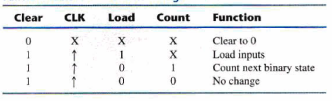
script async='async' crossorigin='anonymous' src='https://pagead2.googlesyndication.com/pagead/js/adsbygoogle.js?client=ca-pub-6016566166623052'/> Verilog coding: April 2020

Sunday, 26 April 2020

Ripple Counter

Verilog HDL for Ripple Counter:

Here is an example of Verilog code for a ripple counter, which is a type of counter that uses a single clock input to increment the count value: 

fpga verilog code example

Example#1

module ripple_counter(input clk, input rst, output reg [3:0] count);

always @(posedge clk) begin
    if (rst)
        count <= 4'b0000;
    else
        count <= count + 1'b1;
end

endmodule


This code defines a module called "ripple_counter" that has a 4-bit output (count) and two inputs: a clock input (clk) and a reset input (rst). The always block is triggered on the rising edge of the clock input and increments the count value by 1 on each rising edge of the clock. The if-else statement checks the reset input, if it is high the count is reset to zero.

The output will be the count value of the ripple counter. The count value will increment every clock cycle until it reach the maximum value of the count register. It's important to note that ripple counters are not recommended for high-frequency or high-speed applications as the propagation delay of the output stage causes the output to change at different times for each bit, resulting in glitches and inaccuracies.


Example# 2

!timescale 1ns/100 ps
module Ripple-Counter_4bit (A3, A2, Al, A0, Count, Reset);
output  A3, A2, Al, A0;
input    Count, R~set;
// Instantiate complementing flip-flop
Comp_D_flip_flop F0 (A0, Count, Reset);
Comp_D_flip_flop Fl (A1, A0, Reset);
Comp_D_flip_flop F2 (A2, A1 , Reset);
Comp_D_flip_flop F3 (A3, A2, Reset);
endmodule
// Complementing flip-flop with delay
// lnput to D flip-flop = Q'
module Comp_D_flip_flop (Q, CLK, Reset);
output   Q;
Input    CLK, Reset;
reg        Q;
always @  (negedge CLK, posedge Reset)
If (Reset) Q <= 1 'b0;
else Q <= #2 ~Q;                       //Intra-assignment delay
endmodule
// Stimulus for testing ripple counter
module t_Ripple_Counter_4bit;
reg Count;
reg Reset;
wire A0, Al , A2 A3;
// Instantiate ripple oounter
Rippte_Counter_4bit M0 (A3, A2, At, A0, Count, Reset);
always
#5 Count = ~Count;
lnitial
    begin
       Count = 1'b0;
       Reset = l'bl;
      #4 Reset = l'b0;
end
initial#170 $finish;

endmodule

Four-bit binary counter with parallel load


Graphical Symbol of Four-bit binary counter with parallel load

Four-bit binary counter with parallel load

Functional Table of Four-bit binary counter with parallel load


fpga verilog code example
Verilog HDL of Four-bit binary counter with parallel load
module Bin-Counter-4bit-Par_Load (
output reg   [3: 0]  A-count,                    // Data output
output          C-out,                                  //Output any
input            [3: 0] Data-in,                      // Data input
input            Count,                                  //Active high to count
                      Load,                                   //Active high to load
                      CLK,                                   // Positive-edge sensitive
                      Clear                                   //Active low  
);
assign      C-out = Count & (~Load) & (A_count == 4'b111l);
always @ (posedge CLK, negedge Clear)
If (~Clear)                          A_count <= 4'b0000;
else If (Load)                      A_count <= data-in;
else If (Count)                    A_count  <= A_count + l'bl;
else                                     A_count <= A_count;            //redundant statement
endmodule


D- Flip Flop Verilog HDL

A D-  Flipflop is the simplest example of a sequential machine. Verilog HDL describes 2-positive edge D- flip-flops in two different modules. The first responds only to the clock signal Clk, the second includes an asynchronous signal reset input rst. Output Q must be declared as a register reg data type in
addition to being listed as an output. Because in a procedural assignment statement, it is a target output. The keyword posedge endures that the transfer of input D into Q is synchronized by the positive-edge transition of Clk. A change in D input at any other time does not change in Output Q.
Positive and Negative Edge D flipflop
The 2nd module includes an Asynchronous reset input, in addition to the synchronous
clk. A specific form of an if statement is used to describe such a flip-flop so that the model
can be synthesized by a software tool. The event expression in the always statement after the @ symbol may have any number of edge events, either posedge or negedge. For modelling hardware,
one event must be a clock event. The other events specify conditions under
which asynchronous logic is to be executed. The flip flop designer knows which signal is the clock signal, but the clock is not an identifier that software tools automatically recognize, as the synchronizing signal of a flip flop circuit. The software tool must be able to conclude which signal is the clock signal, so you need to write the description in a way that enables the software tool to conclude the clock signal correctly, The rules are simple to follow:
( 1) Each if or else if statement in the procedural assignment statements is to correspond to an asynchronous event, (2) the last else statement cornponds to the clock event, and (3) the
asynchronous events are tested first. Thm am two edge events in the second duk of HDL D flip-flop. The negedge rst (reset) event is asynchronous, since it matches the if (-rst) statement. As long as reset signal rst is 0, output Q is cleared to 0. If Clock signal Clk has a positive transition, its effect is
blocked only if reset signal rst is logic 1 can the posedge clock event synchrounously transfer Input D into Output Q.

D- Positive edge triggered flip-flop

Master-Slave D flip-flop


fpga verilog code example

HDL Verilog of D flipflop
// D flip-flop without reset
module D-Flip (Q, D, Clk);
output Q;
input D, Clk;
reg Q;
always @ (posedge Clk)
Q <= D;
endmodule

// D flipflop with asynchronous reset

module DFlip (output reg Q, input D, Clk, rst);
always @ (posedge Clk, negedge rst)
If (-rst) Q <= I'b0;          // Same as: if (rst == 0)
else Q <= D;
endmodule

D-Latch Verilog code:

The D-latch is a transparent and responds to a change in data input with a change in output, as long as
the enable input is high. It has one output Q and  two inputs, D and en. Since Q is evaluated in a procedural statement, it must be declared as register type. D-latch responds to input signal levels, so the two inputs are listed without edge qualifiers in the event enable expression following the @ symbol in the always statement. it has only one blocking procedural assignment statement and it also specifies the transfer of D-input to Q-output if logic 1 i.e when enable is true. This statement is executed every time when there is a change in input D if enable is  logic1.
D-Latch Gate level and truth Table.
D-Latch Graphical Symbol.
fpga verilog code example
Verilog of D latch

module D-latch (Q, 0, en); // en is enable
output Q;
Input D, en;
reg Q;
always @ (en or D)
If (en) Q <= D;   //Same as: If (enable == 1)
endmodule


// Alternative syntax 
module D-latch (output reg Q, input enable, D);
always @ (enable, D)
If (enable) Q <= D;   // No action if enable not asserted
endmodule


Here is an example of VHDL code for a D-latch:


library IEEE; use IEEE.STD_LOGIC_1164.ALL; entity D_latch is Port ( D : in STD_LOGIC; clk : in STD_LOGIC; Q : out STD_LOGIC); end D_latch; architecture Behavioral of D_latch is begin process(clk) begin if (clk'event and clk = '1') then Q <= D; end if; end process; end Behavioral;

And here is an example of Verilog code for a D-latch:


module D_latch (input D, clk, output reg Q); always @(posedge clk) begin Q <= D; end endmodule


Both codes define a D-latch module with inputs D and clk, and an output Q. The D-latch is a level sensitive device and uses the input D as the data input, and the input clk as the enable input.

In the VHDL code, the process is sensitive to the clock input and the output Q is assigned the value of the input D when there is a rising edge on the clock input.

In the Verilog code, the always block is triggered on the rising edge of the clock input and assigns the value of the input D to the output Q.

Both codes implements the same functionality and are equivalent. Please note that this is a basic example and the actual code may depend on the specific requirements of your design.

Wallace Tree Reduction Technique

Multipliers have gained the significant importance with the introduction of the digital computers. Multipliers are most often used in digital signal processing applications and microprocessors designs. In contrast to process of addition and subtraction, multipliers consume more time and more hardware resources. With the recent advances in technology, a number of multiplication techniques have been implemented for fulfilling the requirement of producing high speed, low power consumption, less area or a combination of them in one multiplier. Speed and area are the two major constraints which conflict each other. Therefore, it is the designer’s task to decide proper balance in selecting an appropriate multiplication technique as per requirements. Parallel multipliers are the high speed multipliers. Therefore, the enhanced speed of the multiplication operation is achieved using various schemes and Wallace tree is one of them.

There are three phases in the multiplier architecture:
1. The first phase is the generation of partial products.
2. Accumulation of partial product in second phase.
3. The third phase is the final addition phase.

Wallace multiplier is an efficient parallel multiplier. In the conventional Wallace tree multiplier, the first step is to form partial product array (of 𝑁2 bits). In the second step, groups of three adjacent rows each, is collected. Each group of three rows is reduced by using full adders and half adders. Full adders are used in each column where there are three bits whereas half adders are used in each column where there are two bits. Any single bit in a column is passed to the next stage in the same column without processing. This reduction procedure is repeated in each successive stage until only two rows remain. In the last step, the remaining two rows are added using a carry propagating adder. An example of a representation of the conventional 8-bit by 8-bit Wallace tree multiplier is shown in Fig. 1. The three row groupings are shown .
Figure 1. Conventional 8-bit by 8-bit Wallace Reduction
Hardware Implementation:
A below figure show 6x6 multipler hardware.